Image of the Week Gallery
Finite Element Analysis for High Temperature In Situ Silicon Carbide MEMS Device
Media Details
Created 8/17/2011
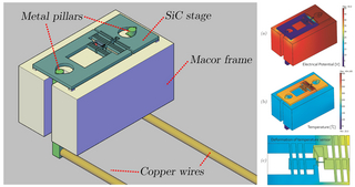
The larger image on the left depicts a three-dimensional schematic of the silicon carbide MEMS device. The stage is designed for in situ mechanical tests in a scanning electron microscope. It allows for the uniaxial testing of micro/nano scale samples (100nm - 10um) in wide temperature range (room temperature to 1000 C) with simultaneous force, strain, and temperature measurements. The three smaller images on the right, labeled a, b, & c are screenshots from finite element analysis conducted using COMSOL software in the Visualization Laboratory. These representations correspond to (a) electrical, (b) thermal, and (c) mechanical responses of the system at 50 V.
Credits
- Wonmo Kang , Mechanical Science & Engineering, UIUC